- Rendszergazda topic
- Crypto Trade
- Facebook profil letiltás kapcsolt ismeretlen Instagram fiók miatt
- Betelik a pohár: nagy igény lenne a gyorshajtás-ellenes technológiára
- Telekom otthoni szolgáltatások (TV, internet, telefon)
- Windows 10
- Otthoni hálózat és internet megosztás
- Vírusirtó topic
- Facebook és Messenger
- Hálózati / IP kamera
Új hozzászólás Aktív témák
-

Ueda
senior tag
Szvsz ennyire nem fogyaszt sokat egy gyorsítótár.
Nem tudom ... nekem ilyen tapasztlatom van :
Engemet meglepett (helyesebben mondva zavart) a megnövekedett hőtermelés és fogyasztás, amikor Q8200 -ről Q9650 -re váltottam. Azt gondoltam, hogy a kisebb teljesítményű modellek eleve a rosszabb csipekből kerülnek ki. Ehhez képest a Q8200 jégcsap volt a Q9650 -hez képest. 4 MB vs 12 MB L2 cache. Szerintem az optimális a 8 MB L2 volt, ami a Q6600 -ban volt.
OS : EndeavourOS KDE . . . . . . Parancs menü : https://pastebin.com/u/txt444
-

S_x96x_S
őstag
>> "és frekvencia regresszió ott már túl nagy lett volna"
> Szvsz ennyire nem fogyaszt sokat egy gyorsítótár.jó kérdés ..
az én megértésem (~spekulációm) szerint -
ez alapján:
https://www.anandtech.com/show/16725/amd-demonstrates-stacked-vcache-technology-2-tbsec-for-15-gaming ( May 31, 2021 )valamennyivel biztosan többet fogyaszt,
-mivel a technológiából eredően egymásra vannak pakolva ..
és így a hőtermelés elvezetése nem olyan egyszerű.
-És még ha le is van kapcsolva[1] .. fizikiailag az is akadályozza (~rontja) a hő elvezetését - az alsó rétegből[2]
-nem egy sikban van az extra cache .. hanem valami felett [3]
és ugyanakkora alapterületen több hő keletkezik.
- És a nagyobb (>200x ) interconnect density [4] - hőelvezetési problémához vezet.
- és ez még csak 2 réteg. [5][1] "The V-Cache is address striped with the normal L3 and can be powered down when not in use. The V-Cache sits on the same power plane as the regular L3."
[2] "The other element is thermals – usually you want the logic on the top die to manage the thermals better as it is close to the heatspreader/heatsink, but moving logic further away from the substrate means that power has to be transported up to the top die. Intel is hoping to mix microbumps and TSVs in upcoming technologies, and TSMC has a similar roadmap for the future for its customers."
[3]
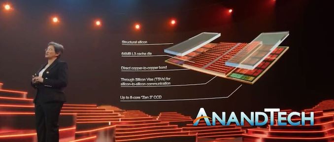
[4] "this packaging enables a >200x interconnect density"[5] "Starting with the technology, this is clearly TSMC’s SoIC Chip-on-Wafer in action, albeit with only two layers. TSMC has demonstrated twelve layers, however those were non-active layers.
The problem with stacking silicon is going to be in the activity,
and subsequently thermals .
We’ve seen with other TSV stacked hardware, like HBM, that SRAM/memory/cache is the perfect vehicle for this as it doesn’t add that much to the thermal requirements of the processor. The downside is that the cache you stack on top is little more than just cache."[ Szerkesztve ]
Mottó: "A verseny jó!"


Új hozzászólás Aktív témák

- Samsung Galaxy S23 128gb - Makulátlan, akár beszámítással
- AKCIÓZVA! HP EliteBook 850 G7 Fémházas Szuper Strapabíró Laptop 15,6" -65% i7-10610U 32/1TB FHD HUN
- AKCIÓZVA! HP EliteBook 850 G7 Fémházas Szuper Strapabíró Laptop 15,6" -65% i7-10610U 32/512 FHD HUN
- Bontatlan Új BOSE QuietComfort Ultra Headphones, bézs-aranyLimitált kiadás
- ASUS TUF Gaming FX505DU Ryzen 7 3750H GTX 1660 Ti 6GB 16GB DDR4 512GB SSD + 1TB HDD 120Hz Full HD
- Eladó komlett konfig+monitor+G923+állvány
- Asus TUF GAMING NVIDIA RTX 3060 6gb i5-11400H 16gb ram 500gb ssd win11
- Munkagép Fujitsu FULL-HD Intel i7-2720qm 8gb ram 256gb ssd / Nvidia 2gb dedikált Win10
- Acer SWIFT vékony 14col Full-HD IPS Intel i5-8250u 4gb ddr4 256gb ssd HDMI Kamera windows11
- EVGA GeForce GTX 1660 SUPER SC ULTRA GAMING 6GB GDDR6 ÁFÁs számlával, kellékszavatossággal